Randy Frank, Contributing Editor -- Design News, June 5, 2006
When Nokia and Amkor Technology discussed 3D packaging roadmaps five years ago, the stage was set for a new packaging solution for logic plus memory integration. Today known as Packaging on Packaging or PoP, the 3D solution addresses a wide range of multimedia applications to integrate digital baseband, application or image processors with high capacity or combination memory devices. By dealing directly with the system supplier, Amkor gained a better understanding of the total requirements (technical, business and logistical) necessary to develop a highly successful product and supply chain infrastructure. The benefits of PoP are being widely recognized in portable applications as PoP is being designed into digital cameras, portable medial players and mobile gaming, in addition to mobile phones.
The industry shift to smart phones with new multimedia features such as web access, camera, video, music and gaming requires a huge increase in processing power and memory capacity. To integrate these costly new features with an expanding processor and memory architecture, the size, weight and cost reduction trends for mobile phones flattened or reversed. The market pays a premium for the right features and functions in innovative form factors. To achieve the design flexibility and cost objectives phone designers have turned to PoP to solve their logic + memory integration challenges, as there are multiple advantages in stacking the memory right on top of the processor.
Previously this stacking was done at the package level with die stacked in a single package. However, stacked die integration has several technical and business issues to overcome. "The processor suppliers are not in the memory business and the memory suppliers are not in the logic business, the business model for stacked die is horrible from all perspectives," says Lee Smith, senior director business development, Amkor Technology.
The method of die stacking known as System in Package or SiP, integrates one or more memory devices into a single package sold by the processor supplier. This approach requires two competing companies to cooperate. The memory supplier has to provide known or near good die in wafer form at near commodity prices and absorb much of the risk for final yields, test and lost revenue from not quite good enough devices on the wafer. From the business perspective, this approach is not flexible or cost-effective for the OEM when sourcing, time to market, design changes and total cost of ownership are taken into account.
To develop the new package stack, Amkor did the package design, development and qualification while Nokia did the package stacking and board level solder joint qualification as reported at ECTC in 2003. Once the PoP was pre-qualified, it was designed into an innovative new phone form factor and specified to the processor and memory semiconductor suppliers to deploy in production.
A key objective in JEDEC and in PoP adoption is defining a flexibly memory interface that supports multiple memory combinations and is supported by all the key memory suppliers as a standard. These standards enable the logic supplier to better floor plan her processor's memory controllers and interconnect interface as a design for stacking which can reduce the package wiring density to reduce cost and improve electrical performance. Current processors are designed for CSPs to interface to a memory Multi-Chip Package (MCP) adjacent on the mother board, as a result the memory interface bond pads are on one side of the chip which pushes wiring density into the bottom logic package to reroute the crossing memory circuits from the top four-sided package
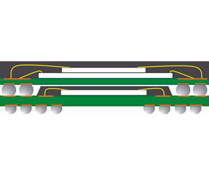
To deploy PoP stacks in high volume, a key design challenge is controlling warpage of the bottom package across high temperature lead-free solder reflow profiles. As a result, the mold compound for the top and bottom packages are not necessarily the same. Because the bottom package has an unbalanced construction, the compound is specifically selected for warpage control. "When you mold all the way to the package edges and saw singulate like the top MCP, that's much easier to control warpage and coplanarity," says Smith. "With the unbalanced package, the substrate is thicker than the mold cap, so the coefficients of thermal expansion (CTE) and modulus of elasticity of the materials become more important."
Another key aspect to address warpage was shifting the industry from looking at room temperature coplanarity as the critical criteria for incoming inspection. Since the warpage factors with two packages are most critical at the liquidus temperature where the two units solder together, this changed to characterizing the two packages together for the warpage profile across the reflow temperature profile. This shift in industry thinking has proven to be effective. "Stacking yields are being reported from OEMs at high levels matching what they get with 0.5 mm CSP assembly," notes Smith.
The first PoP stack for cellphones went into production in October 2004. The PoP stack had four elements in the top package — SDRAM, NOR and NAND die plus a spacer. "When you get to complex four and five stacks with low cumulative die yield and high die and test cost, then PoP overwhelmingly becomes the lowest cost solution," says Smith.
The outlook for the market acceptance for PoP products is extremely good. Jan Vardeman of market research company TechSearch International forecasts 300 million packaging stacks for 2007. Part of this optimism is based on equipment suppliers either optimizing or retrofitting their equipment for package stacking. "The EMS/OEM guys are quickly coming on board," says Smith. "Flextronics has been doing this in high volume assembly for a couple of years. By next year this will become a dominant technology for logic plus memory integration."
Contact: Lee Smith, senior director business development, Amkor lsmit@amkor.com

