Sunday, September 23, 2007
IC Packaging
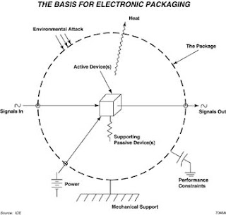
In order for the active device to function, it must be electrically connected to other devices-with physical assurance that the connections will be maintained. Further, the active device must be protected from attack by the environment. Finally, since the active device consumes power to perform its function, heat is generated. Since heat can shorten the life of active devices, a means must be provided to carry the heat away.
To provide these necessary functions of interconnection, physical support, environmental protection and heat dissipation, the active device must be surrounded by or encased in a package. An illustrarion of this concept is presented in Figure 1. Packages may be simple or they maybe complex-depending on the nature of the device, the system of which it is a part and the environment in which the device must operate.
The very surrounding of the active device with protective material, however, can degrade the performance if the device, increase its physical size and weight, make testing the device more difficult and decrease reliability. Moreover, the art of
making the electronic package incure costs-which may be far higher than the cost of the active device itself. Thus, the art of providing an effective electronic package becomes a complex balence of providing desired functions against constraints which may interact among themselves as even further constraints.
As a practical matter, the IC manufacturer must decide whether to package a given IC in one or more standard packages (nesessary for merchant sales) or develop one unique to its needs (giving it a systems advantage over its competitors). We will confine our discusions to "standard" types, however.
Sunday, September 16, 2007
What is wire bonding
Wire bonding is a method of making interconnections between a microchip and other electronics as part of semiconductor device fabrication.
The wire is generally made up of one of the following:
Wire diameters start at 15 µm and can be up to several hundred micrometres for high-powered applications.
There are two main classes of wire bonding:
Ball bonding usually is restricted to gold and copper wire and usually requires heat. Wedge bonding can use either gold or aluminium wire, with only the gold wire requiring heat.
In either type of wire bonding, the wire is attached at both ends using some combination of heat, pressure, and ultrasonic energy to make a weld.
Wire bonding is generally considered the most cost-effective and flexible interconnect technology, and is used to assemble the vast majority of semiconductor packages.
Category: SemTuesday, September 11, 2007
What is Flip Chip
What is Flip Chip?
Flip Chip (FC) is not a specific package (like SOIC), or even a package type (like BGA). Flip Chip describes the method of electrically connecting the die to the package carrier. The package carrier, either substrate or leadframe, then provides the connection from the die to the exterior of the package. In "standard" packaging, the interconnection between the die and the carrier is made using wire. The die is attached to the carrier face up, then a wire is bonded first to the die, then looped and bonded to the carrier. Wires are typically 1-5 mm in length, and 25-35 µm in diameter. In contrast, the interconnection between the die and carrier in flip chip packaging is made through a conductive "bump" that is placed directly on the die surface. The bumped die is then "flipped over" and placed face down, with the bumps connecting to the carrier directly. A bump is typically 70-100 µm high, and 100-125 µm in diameter.
The flip chip connection is generally formed one of two ways: using solder or using conductive adhesive. By far, the most common packaging interconnect is solder Current solder types are: eutectic (63%Sn, 37%Pb) or high lead (95%Pb, 5%Sn) or lead-free (97.5%Sn, 2.5%Ag) compositions. The solder bumped die is attached to a substrate by a solder reflow process, very similar to the process used to attach BGA balls to the package exterior. After the die is soldered, underfill is added between the die and the substrate. Underfill is a specially engineered epoxy that fills the area between the die and the carrier, surrounding the solder bumps. It is designed to control the stress in the solder joints caused by the difference in thermal expansion between the silicon die and the carrier. Once cured, the underfill absorbs the stress, reducing the strain on the solder bumps, greatly increasing the life of the finished package. The chip attach and underfill steps are the basics of flip chip interconnect. Beyond this, the remainder of package construction surrounding the die can take many forms and can generally utilize existing manufacturing processes and package formats.
Benefits of Flip Chip:
Using flip chip interconnect offers a number of possible advantages to the user: